

Field Emission Scanning Electron Microscope YF-2800
The YF-2800 scanning electron microscope (SEM) has excellent low-voltage and high-resolution imaging capabilities, and is equipped with a thermal field emission electron gun (Schottky FEG) to obtain high resolution while ensuring the stability of the beam current. Advanced full in-column automatic acceleration & deceleration technology integrated into the electron optical column ensures outstanding imaging perrormance at low accelerating voltages. The design of electromagnetic-electrostatic compound immersion objective lens further enhances the high-resolution imaging capability of the system. The optimized detection system can efficiently collect secondarr electron and backscattered electron signals at low voltage, which can directly observe non-conductive samples at low voltage, reduce the irradiation damage to the sample, and reveal the surfrace micromorphology and structure information.
Classification:
Scanning Electron Microscope
Core advantages
Product Advantages

Excellent Expansion Ability

User Interface
- 产品描述
- 用户界面
- 性能参数
- 应用案例
-
- Commodity name: Field Emission Scanning Electron Microscope YF-2800
The YF-2800 scanning electron microscope (SEM) has excellent low-voltage and high-resolution imaging capabilities, and is equipped with a thermal field emission electron gun (Schottky FEG) to obtain high resolution while ensuring the stability of the beam current. Advanced full in-column automatic acceleration & deceleration technology integrated into the electron optical column ensures outstanding imaging perrormance at low accelerating voltages. The design of electromagnetic-electrostatic compound immersion objective lens further enhances the high-resolution imaging capability of the system. The optimized detection system can efficiently collect secondarr electron and backscattered electron signals at low voltage, which can directly observe non-conductive samples at low voltage, reduce the irradiation damage to the sample, and reveal the surfrace micromorphology and structure information.
Product Advantages
Excellent Expansion Ability
-
· Clear and concise interface layout
· Ergonomic keyboard design
· Equipped with multiple safety interlocks
· Simple and smooth operation

-
Kernel parameters Resolution 0.6nm@15kV(SE) 1.8nm@1kV(SE) Accelerating voltage 0.02-30kV Magnification 1~2500000x Gun type Schottky FEG Objective lens Electromagnetic-electrostatic compound immersion objective lens Probe current 1pA~20nA Detector and expansion equipment Standard configuration ET detector Inlens detector Optional configuration Electric retractable BSD detector Low-voltageBSD detector STEM detector Plasma cleaner Specimen chamber Chamber 340mm inner diameter, 260mm height Multiple accessory ports for EBSD, EDS, CL, etc. Sample exchange chamber is optional. Specimen stage 5-axes automatic stage X、Y=125mm,Z=50mm,R=360°cont.,T=-5°~+70° Image system Dual cameras (Top-view and side-view camera) Software Language Chinese/English, other languages can be customized System Windows Automatic functions Automatic gun alignment,automatic aperture alignment, automatic focus/stigmation,automatic brightness/contrast, etc. Other functions Split screen display,image annotation,scan rotation, image measurement,tilt compensation,etc. -

Carbon nanotubes

Graphene

HfO2 / SiC ceramic

Stainless steel

Lithium iron phosphate positive electrode sheet
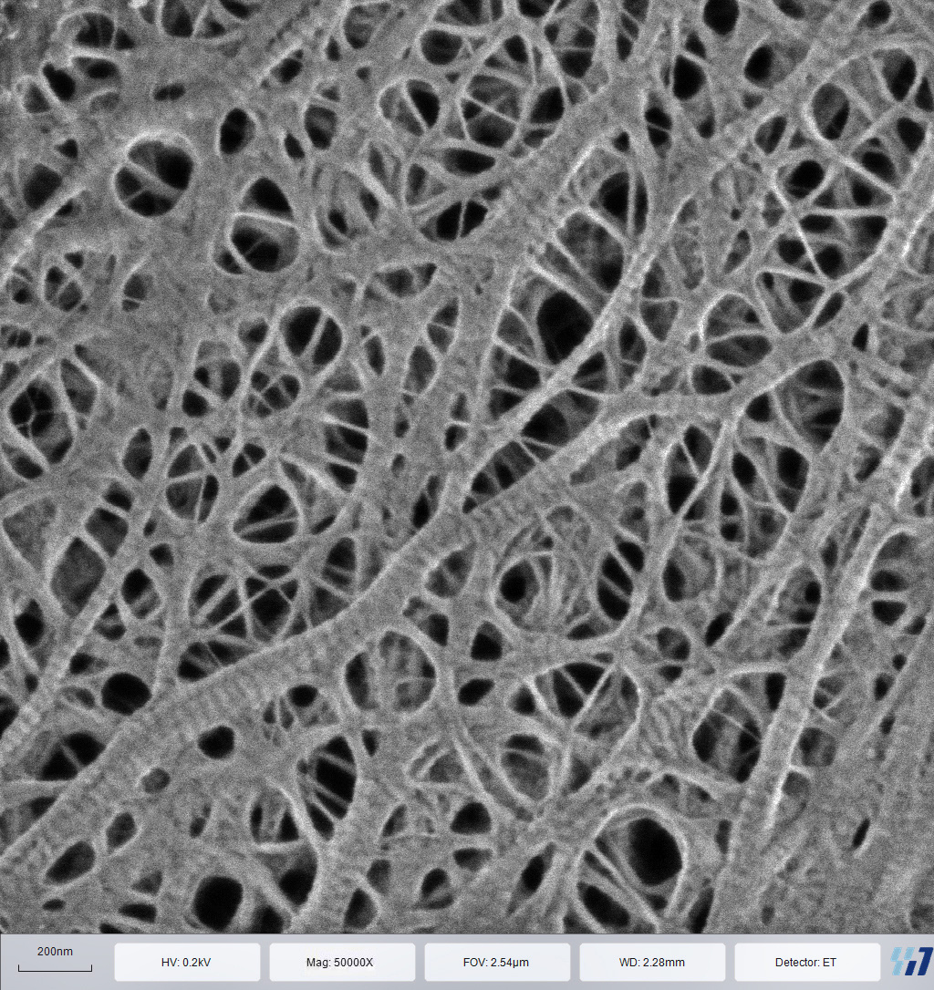
Wet stretch film

Silicon-carbon anode material

Nickel metal

Memory chip

Multilayer ceramic capacitor (MLCC)

Electron beam exposure etching pattern

Hard alloy

Brain tissue

Mouse lung tissue

Liver tissue

Glomerulus
Performance parameters
- 产品描述
- 用户界面
- 性能参数
- 应用案例
-
- Commodity name: Field Emission Scanning Electron Microscope YF-2800
The YF-2800 scanning electron microscope (SEM) has excellent low-voltage and high-resolution imaging capabilities, and is equipped with a thermal field emission electron gun (Schottky FEG) to obtain high resolution while ensuring the stability of the beam current. Advanced full in-column automatic acceleration & deceleration technology integrated into the electron optical column ensures outstanding imaging perrormance at low accelerating voltages. The design of electromagnetic-electrostatic compound immersion objective lens further enhances the high-resolution imaging capability of the system. The optimized detection system can efficiently collect secondarr electron and backscattered electron signals at low voltage, which can directly observe non-conductive samples at low voltage, reduce the irradiation damage to the sample, and reveal the surfrace micromorphology and structure information.
Product Advantages
Excellent Expansion Ability
-
· Clear and concise interface layout
· Ergonomic keyboard design
· Equipped with multiple safety interlocks
· Simple and smooth operation
-
Kernel parameters Resolution 0.6nm@15kV(SE) 1.8nm@1kV(SE) Accelerating voltage 0.02-30kV Magnification 1~2500000x Gun type Schottky FEG Objective lens Electromagnetic-electrostatic compound immersion objective lens Probe current 1pA~20nA Detector and expansion equipment Standard configuration ET detector Inlens detector Optional configuration Electric retractable BSD detector Low-voltageBSD detector STEM detector Plasma cleaner Specimen chamber Chamber 340mm inner diameter, 260mm height Multiple accessory ports for EBSD, EDS, CL, etc. Sample exchange chamber is optional. Specimen stage 5-axes automatic stage X、Y=125mm,Z=50mm,R=360°cont.,T=-5°~+70° Image system Dual cameras (Top-view and side-view camera) Software Language Chinese/English, other languages can be customized System Windows Automatic functions Automatic gun alignment,automatic aperture alignment, automatic focus/stigmation,automatic brightness/contrast, etc. Other functions Split screen display,image annotation,scan rotation, image measurement,tilt compensation,etc. -
Carbon nanotubes
Graphene
HfO2 / SiC ceramic
Stainless steel
Lithium iron phosphate positive electrode sheet
Wet stretch film
Silicon-carbon anode material
Nickel metal
Memory chip
Multilayer ceramic capacitor (MLCC)
Electron beam exposure etching pattern
Hard alloy
Brain tissue
Mouse lung tissue
Liver tissue
Glomerulus
Application Cases
- 产品描述
- 用户界面
- 性能参数
- 应用案例
-
- Commodity name: Field Emission Scanning Electron Microscope YF-2800
The YF-2800 scanning electron microscope (SEM) has excellent low-voltage and high-resolution imaging capabilities, and is equipped with a thermal field emission electron gun (Schottky FEG) to obtain high resolution while ensuring the stability of the beam current. Advanced full in-column automatic acceleration & deceleration technology integrated into the electron optical column ensures outstanding imaging perrormance at low accelerating voltages. The design of electromagnetic-electrostatic compound immersion objective lens further enhances the high-resolution imaging capability of the system. The optimized detection system can efficiently collect secondarr electron and backscattered electron signals at low voltage, which can directly observe non-conductive samples at low voltage, reduce the irradiation damage to the sample, and reveal the surfrace micromorphology and structure information.
Product Advantages
Excellent Expansion Ability
-
· Clear and concise interface layout
· Ergonomic keyboard design
· Equipped with multiple safety interlocks
· Simple and smooth operation
-
Kernel parameters Resolution 0.6nm@15kV(SE) 1.8nm@1kV(SE) Accelerating voltage 0.02-30kV Magnification 1~2500000x Gun type Schottky FEG Objective lens Electromagnetic-electrostatic compound immersion objective lens Probe current 1pA~20nA Detector and expansion equipment Standard configuration ET detector Inlens detector Optional configuration Electric retractable BSD detector Low-voltageBSD detector STEM detector Plasma cleaner Specimen chamber Chamber 340mm inner diameter, 260mm height Multiple accessory ports for EBSD, EDS, CL, etc. Sample exchange chamber is optional. Specimen stage 5-axes automatic stage X、Y=125mm,Z=50mm,R=360°cont.,T=-5°~+70° Image system Dual cameras (Top-view and side-view camera) Software Language Chinese/English, other languages can be customized System Windows Automatic functions Automatic gun alignment,automatic aperture alignment, automatic focus/stigmation,automatic brightness/contrast, etc. Other functions Split screen display,image annotation,scan rotation, image measurement,tilt compensation,etc. -
Carbon nanotubes
Graphene
HfO2 / SiC ceramic
Stainless steel
Lithium iron phosphate positive electrode sheet
Wet stretch film
Silicon-carbon anode material
Nickel metal
Memory chip
Multilayer ceramic capacitor (MLCC)
Electron beam exposure etching pattern
Hard alloy
Brain tissue
Mouse lung tissue
Liver tissue
Glomerulus
Customer service telephone
Enterprise mailbox
Company address
Rooms 101 and 201, Building 11, No 8, Jinfeng Road, Suzhou New District, Jiangsu Province, China
Copyright©2023 Yidon Technologies Co., Ltd. All rights reserved Website Construction:China Enterprise Power Kunshan SEO