

Field Emission Scanning Electron Microscope YF-1801
The YF1801 scanning electron microscope (SEM) uses Schottky field emission gun (FEG) technology. Advanced full-column accelerating technology integrated into the electron optical column ensures outstanding imaging performance at low accelerating voltages, enabling high-resolution imaging of various materials. Multiple detector systems efficiently collect diverse electron signals emitted from the sample for imaging, revealing microscopic morphology and structural information of the sample to the maximum extent.
Classification:
Scanning Electron Microscope
Core advantages
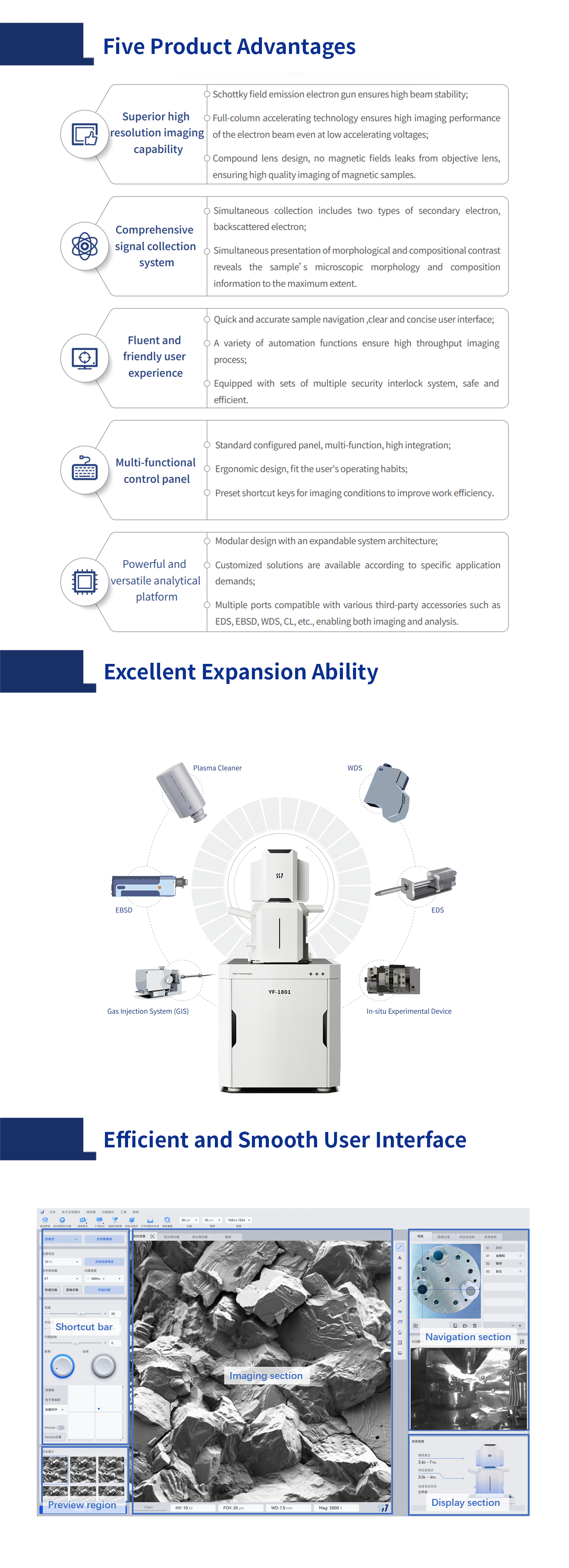
User Interface
- 产品描述
- 用户界面
- 性能参数
- 应用案例
-
- Commodity name: Field Emission Scanning Electron Microscope YF-1801
The YF1801 scanning electron microscope (SEM) uses Schottky field emission gun (FEG) technology. Advanced full-column accelerating technology integrated into the electron optical column ensures outstanding imaging performance at low accelerating voltages, enabling high-resolution imaging of various materials. Multiple detector systems efficiently collect diverse electron signals emitted from the sample for imaging, revealing microscopic morphology and structural information of the sample to the maximum extent.
-
· Clear and concise interface layout
· Ergonomic keyboard design
· Equipped with multiple safety interlocks
· Simple and smooth operation

-
Kernel parameters Resolution 1.0nm@15kV(SE) 1.5nm@1kV(SE) Gun type Schottky FEG Objective lens Compound objective lens combined with electrostatic lens and magnetic lens Probe current 1pA~20nA(100nA Optional configuration) Image size 256*256~16k*16k Detector and expansion equipment Standard configuration ET detector Inlens detector Optional configuration BSD detector STEM detector Plasma cleaner Specimen chamber Chamber 340mm inner diameter, 260mm height Multiple accessory ports for EBSD,EDS,CL,etc. Specimen stage 5-axes automatic stage Maximum sample weight 2.5kg X、Y=125mm,Z=50mm,R=360°cont.,T=-5~70° Image system Dual cameras (Top-view and side-view camera) Software Language Chinese/English System Windows Automatic functions Automatic gun alignment,automatic aperture alignment, automatic focus/stigmation,automatic brightness/contrast, etc. Other functions Split screen display,image annotation,scan rotation, image measurement,tilt compensation,etc. -
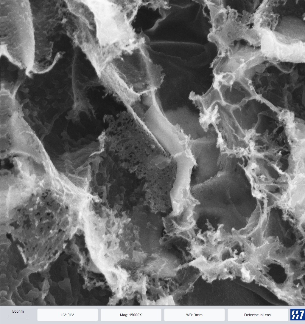
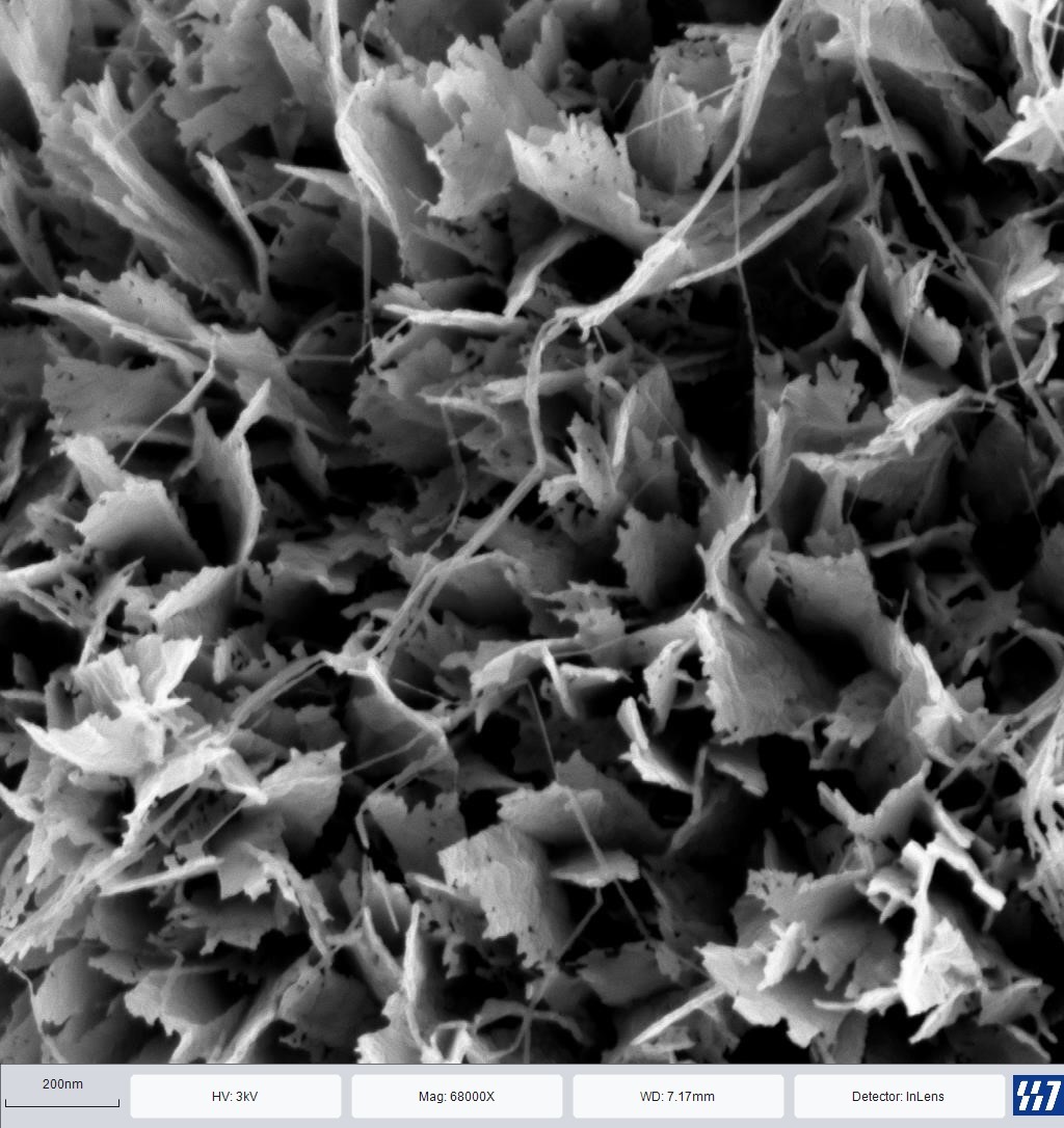
Graphene with porous layered structure
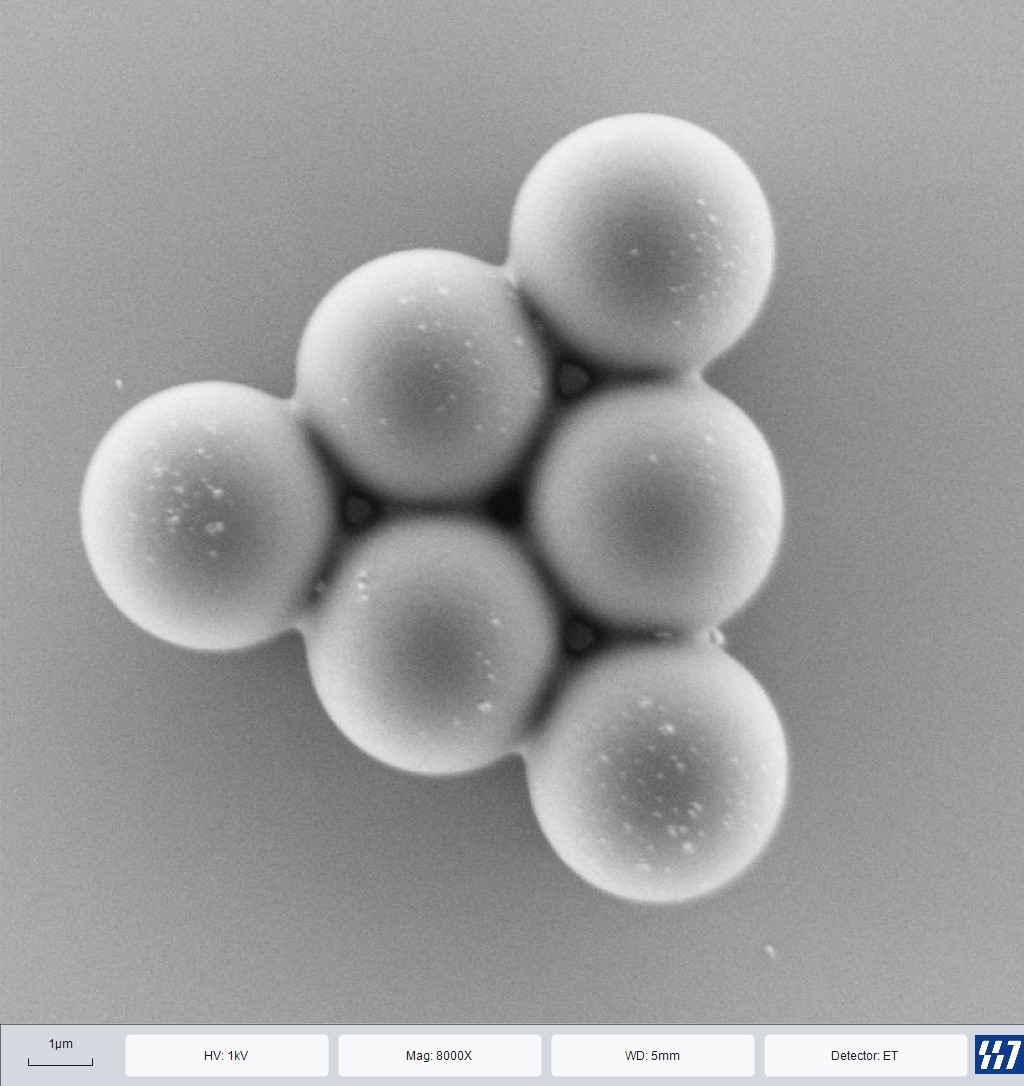
Polymer microspheres
Silicon oxide electrode
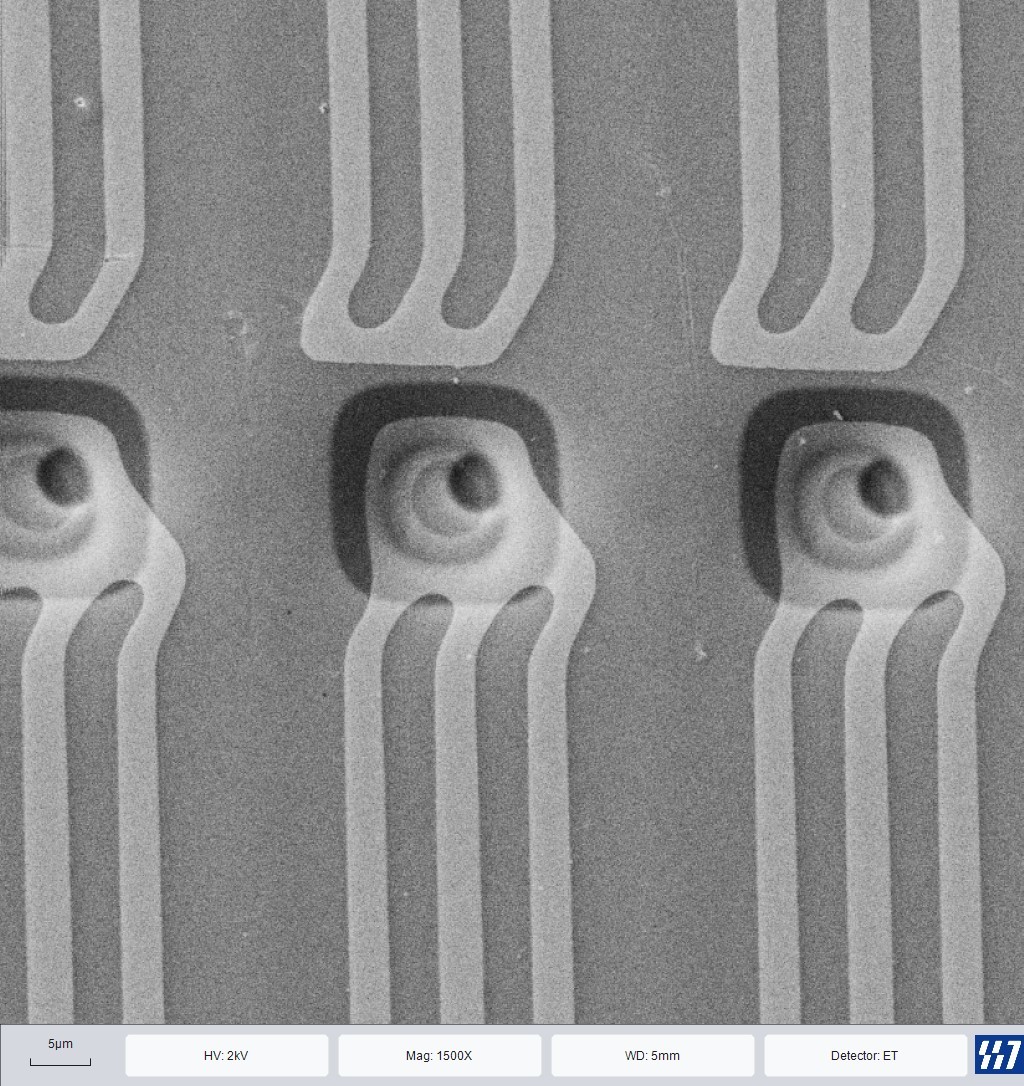
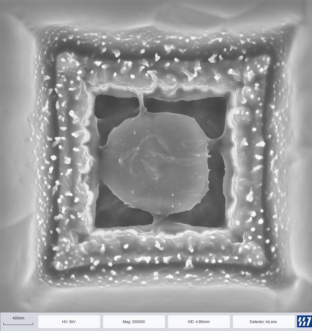
Display pixel unit
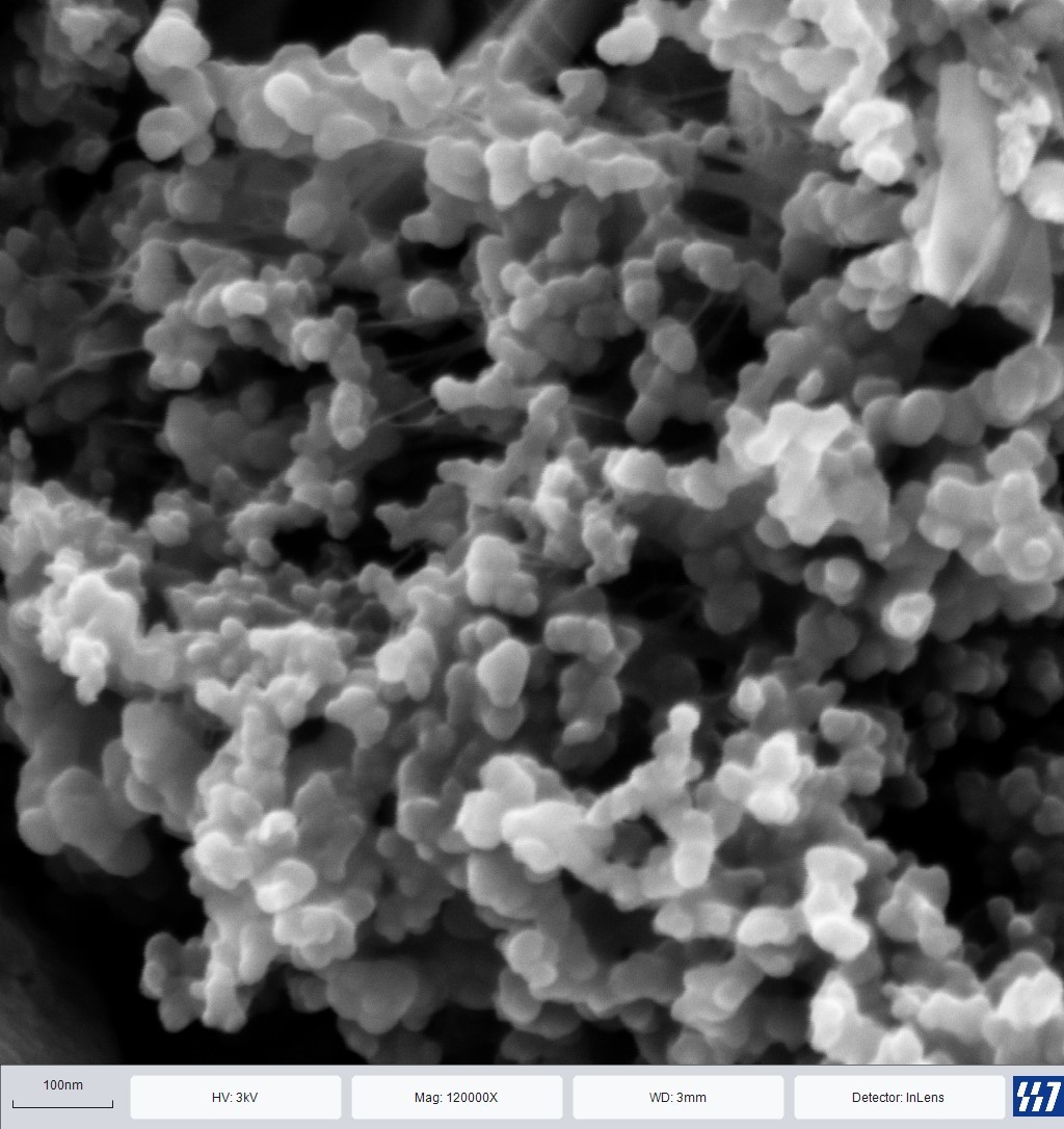
Carbon nanoparticles
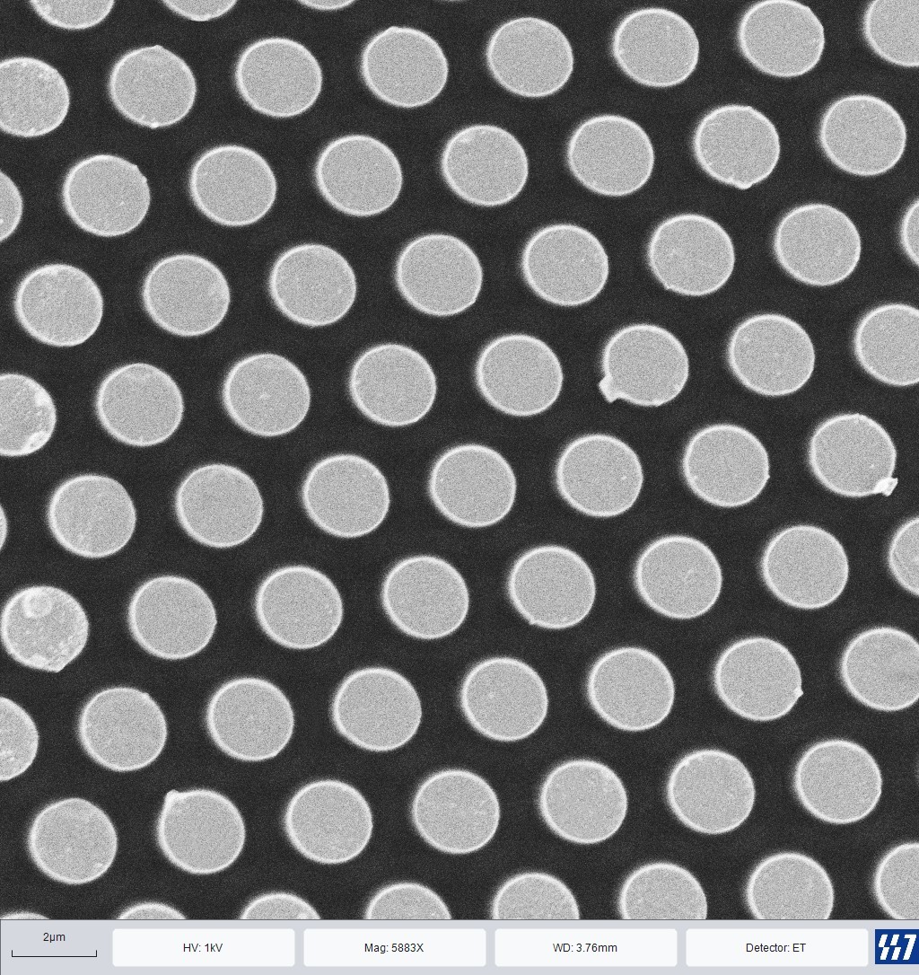
Photoresist array on Al2O3 substrate surface
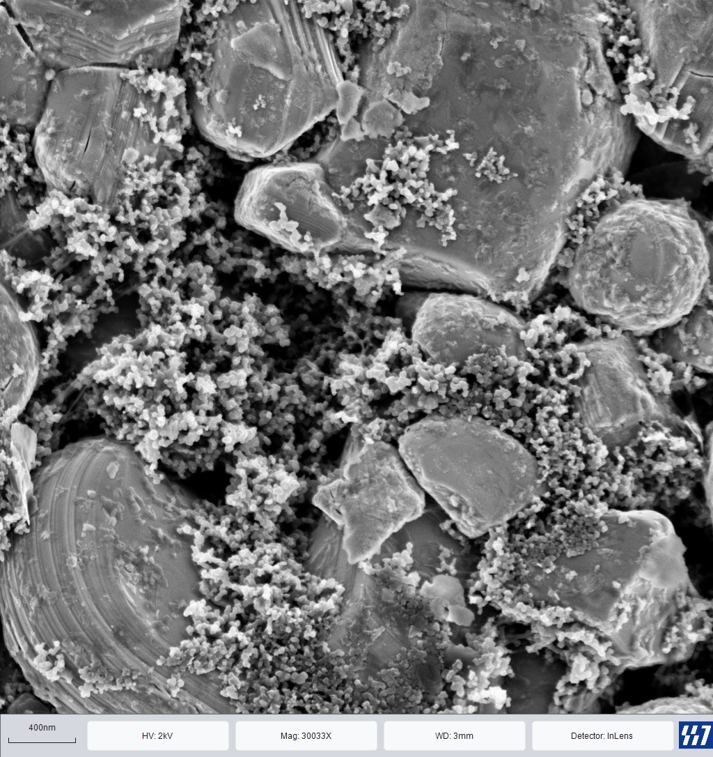
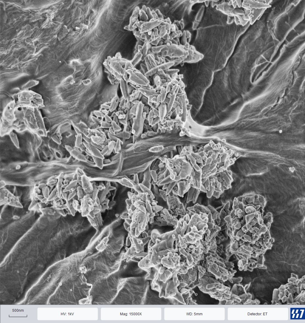
Lithium-ion battery cathode materials
CaCO3 particles on the surface of paper
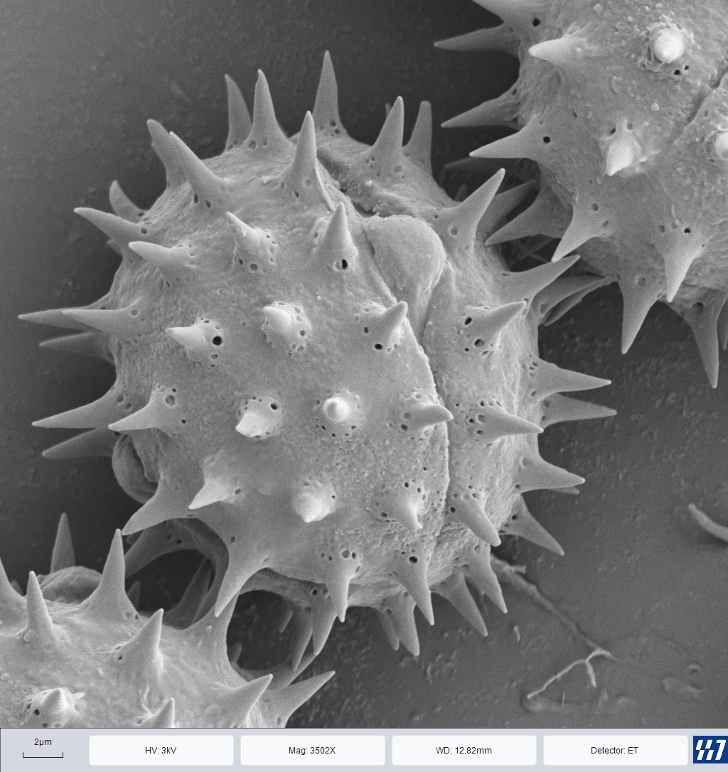
Cosmos bipinnatus pollen
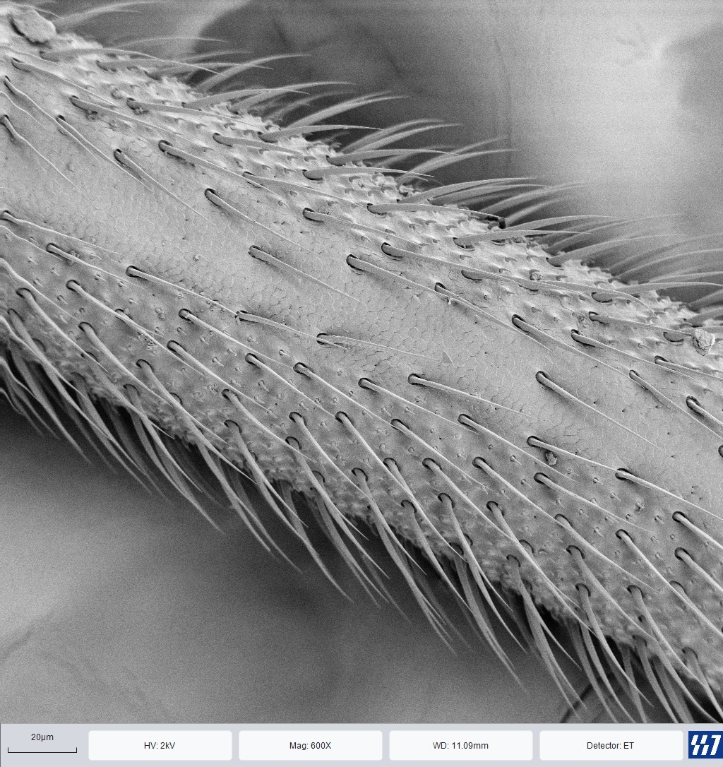
Stag beetle antennal sensilla
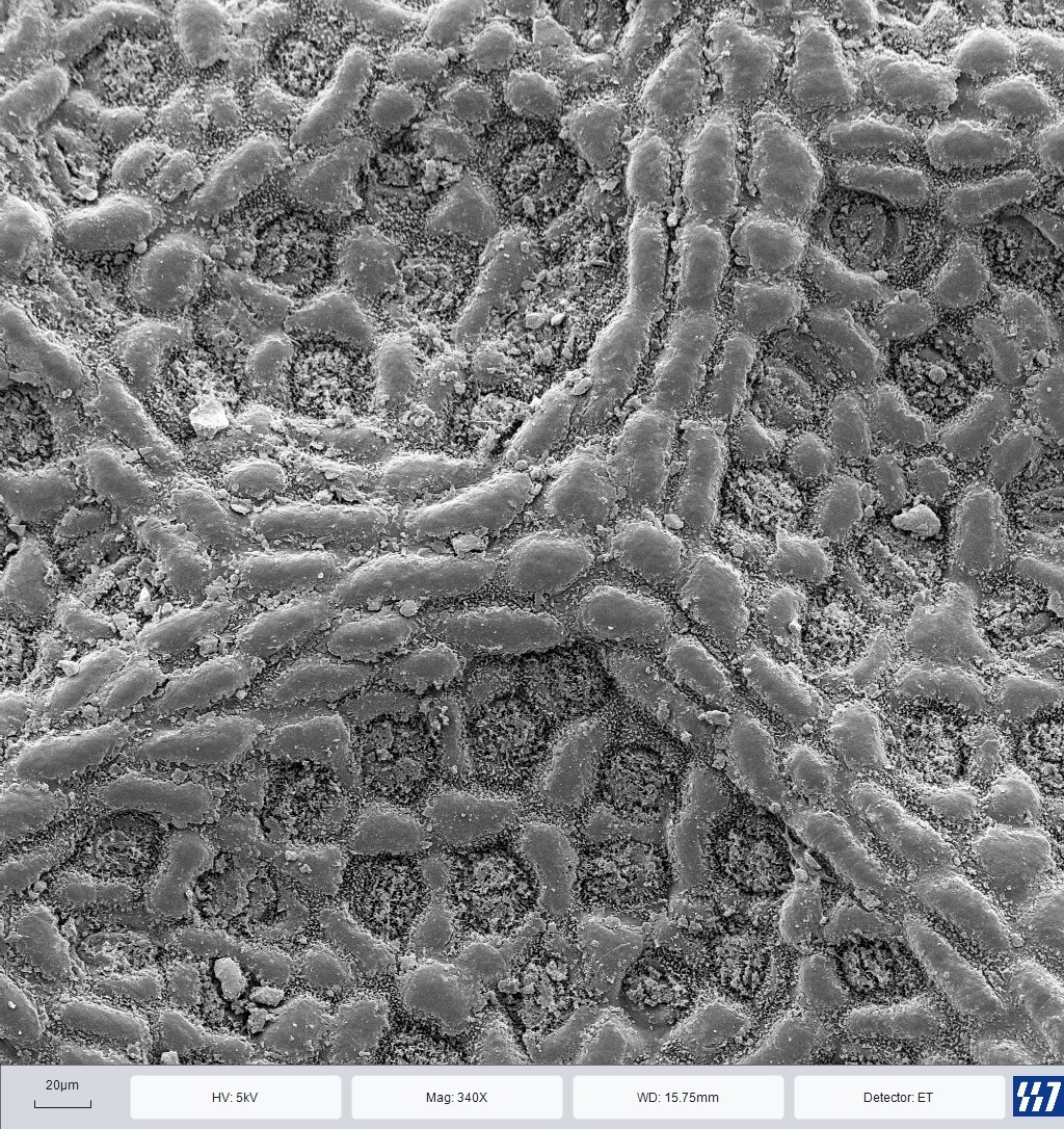
Surface structure of camphor leaves
Titanium oxide nanosheets
Performance parameters
- 产品描述
- 用户界面
- 性能参数
- 应用案例
-
- Commodity name: Field Emission Scanning Electron Microscope YF-1801
The YF1801 scanning electron microscope (SEM) uses Schottky field emission gun (FEG) technology. Advanced full-column accelerating technology integrated into the electron optical column ensures outstanding imaging performance at low accelerating voltages, enabling high-resolution imaging of various materials. Multiple detector systems efficiently collect diverse electron signals emitted from the sample for imaging, revealing microscopic morphology and structural information of the sample to the maximum extent.
-
· Clear and concise interface layout
· Ergonomic keyboard design
· Equipped with multiple safety interlocks
· Simple and smooth operation
-
Kernel parameters Resolution 1.0nm@15kV(SE) 1.5nm@1kV(SE) Gun type Schottky FEG Objective lens Compound objective lens combined with electrostatic lens and magnetic lens Probe current 1pA~20nA(100nA Optional configuration) Image size 256*256~16k*16k Detector and expansion equipment Standard configuration ET detector Inlens detector Optional configuration BSD detector STEM detector Plasma cleaner Specimen chamber Chamber 340mm inner diameter, 260mm height Multiple accessory ports for EBSD,EDS,CL,etc. Specimen stage 5-axes automatic stage Maximum sample weight 2.5kg X、Y=125mm,Z=50mm,R=360°cont.,T=-5~70° Image system Dual cameras (Top-view and side-view camera) Software Language Chinese/English System Windows Automatic functions Automatic gun alignment,automatic aperture alignment, automatic focus/stigmation,automatic brightness/contrast, etc. Other functions Split screen display,image annotation,scan rotation, image measurement,tilt compensation,etc. -
Graphene with porous layered structure
Polymer microspheres
Silicon oxide electrode
Display pixel unit
Carbon nanoparticles
Photoresist array on Al2O3 substrate surface
Lithium-ion battery cathode materials
CaCO3 particles on the surface of paper
Cosmos bipinnatus pollen
Stag beetle antennal sensilla
Surface structure of camphor leaves
Titanium oxide nanosheets
Application Cases
- 产品描述
- 用户界面
- 性能参数
- 应用案例
-
- Commodity name: Field Emission Scanning Electron Microscope YF-1801
The YF1801 scanning electron microscope (SEM) uses Schottky field emission gun (FEG) technology. Advanced full-column accelerating technology integrated into the electron optical column ensures outstanding imaging performance at low accelerating voltages, enabling high-resolution imaging of various materials. Multiple detector systems efficiently collect diverse electron signals emitted from the sample for imaging, revealing microscopic morphology and structural information of the sample to the maximum extent.
-
· Clear and concise interface layout
· Ergonomic keyboard design
· Equipped with multiple safety interlocks
· Simple and smooth operation
-
Kernel parameters Resolution 1.0nm@15kV(SE) 1.5nm@1kV(SE) Gun type Schottky FEG Objective lens Compound objective lens combined with electrostatic lens and magnetic lens Probe current 1pA~20nA(100nA Optional configuration) Image size 256*256~16k*16k Detector and expansion equipment Standard configuration ET detector Inlens detector Optional configuration BSD detector STEM detector Plasma cleaner Specimen chamber Chamber 340mm inner diameter, 260mm height Multiple accessory ports for EBSD,EDS,CL,etc. Specimen stage 5-axes automatic stage Maximum sample weight 2.5kg X、Y=125mm,Z=50mm,R=360°cont.,T=-5~70° Image system Dual cameras (Top-view and side-view camera) Software Language Chinese/English System Windows Automatic functions Automatic gun alignment,automatic aperture alignment, automatic focus/stigmation,automatic brightness/contrast, etc. Other functions Split screen display,image annotation,scan rotation, image measurement,tilt compensation,etc. -
Graphene with porous layered structure
Polymer microspheres
Silicon oxide electrode
Display pixel unit
Carbon nanoparticles
Photoresist array on Al2O3 substrate surface
Lithium-ion battery cathode materials
CaCO3 particles on the surface of paper
Cosmos bipinnatus pollen
Stag beetle antennal sensilla
Surface structure of camphor leaves
Titanium oxide nanosheets
Customer service telephone
Enterprise mailbox
Company address
88, Keling Road, Suzhou New District, Jiangsu Province, 215163, China
Copyright©2023 Yidon Technologies (Suzhou) Co., Ltd. All rights reserved Website Construction:China Enterprise Power Kunshan SEO