

Argon ion field emission scanning electron microscope ABSEM200
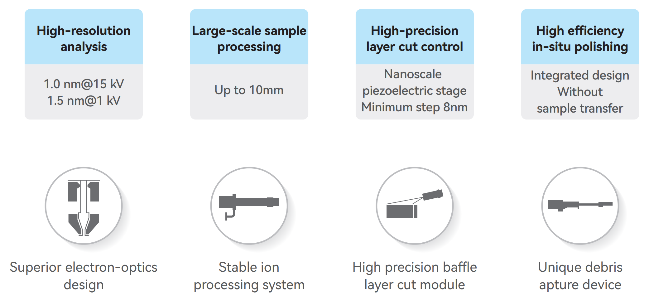
As an innovative multi-functional sample preparation and analysis system,the argon ion beam field emission scanning electron microscope ABSEM 200 has made a breakthrough by integrating a broad-beam argon ion gun into into the scanning electron microscope. It has successfully achieved a seamless connection between ion beam in-situ polishing and high-resolution electron scanning imaging, eliminating sample transfer and greatly enhancing the analysis efficiency. The broad ion beam technology equipped on the ABSEM 200 has powerrul processing capabilities, enabling it to easily handle large-sized samples at the millimeter level, which significantly broadens its application range. The grazing angle design can effectively reduce the damage to samples during the processing, ensuring the integrity and original state of the samples. The nanometer-level layer cutting module can precisely control the layer removal thickness, and the unique debris trapping device ensures the stable operation of the system, effectively avoiding the interrerence of debris on experiments and potential risks.The ABSEM 200 is parricularly suitable for samples that are environmentally sensitive or have complex structures, providing users with an efficient and accurate sample characterization solution. The ABSEM 200 has successfully opened a new chapter in exploring the microscopic world!
Classification:
Product
Scanning Electron Microscope
Core advantages
Technical Principle
|
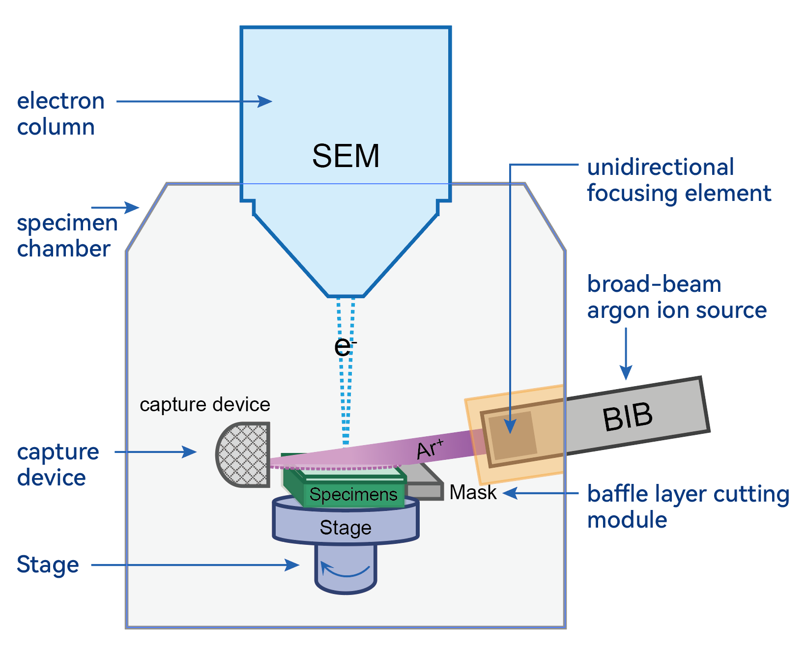
The ABSEM 200 dual beam system integrates the argon ion gun on the Yidon Technologies field emission scanning electron microscope platform, which makes the wide argon ion beam incident on the sample surrace at an adjustable grazing Angle (3-9°), and focuses the ion beam into a linear beam spot through the unidirectional focusing module at the front end to improve the beam density on the sample surface. The energy of the ion beam can be more efffciently applied to the microscopic region of the sample. The swing or rotation of the stage can effectively reduce the curtain effect and minimize the radiation damage of the sample. The ABSEM 200 is also equipped with a high-precision baffle layer cutting module, which can precisely remove the thickness of the sample surface according to the specific needs of the researchers, resulting in the ideal depth of observation and high-resolution resolution. At the same time, the unique debris capture device can effectively collect all kinds of pollutants generated in the ion beam sputtering, ensuring the clean and stable operating environment of the system. After the polishing process, the exposed sample surface can be directly scanned by high-resolution imaging without sample transfer, and the micro-morphology and structure information of the sample surface can be obtained.
|
Product Advantages
User Interface
- 产品描述
- 用户界面
- 性能参数
- 应用案例
-
- Commodity name: Argon ion field emission scanning electron microscope ABSEM200
As an innovative multi-functional sample preparation and analysis system,the argon ion beam field emission scanning electron microscope ABSEM 200 has made a breakthrough by integrating a broad-beam argon ion gun into into the scanning electron microscope. It has successfully achieved a seamless connection between ion beam in-situ polishing and high-resolution electron scanning imaging, eliminating sample transfer and greatly enhancing the analysis efficiency. The broad ion beam technology equipped on the ABSEM 200 has powerrul processing capabilities, enabling it to easily handle large-sized samples at the millimeter level, which significantly broadens its application range. The grazing angle design can effectively reduce the damage to samples during the processing, ensuring the integrity and original state of the samples. The nanometer-level layer cutting module can precisely control the layer removal thickness, and the unique debris trapping device ensures the stable operation of the system, effectively avoiding the interrerence of debris on experiments and potential risks.The ABSEM 200 is parricularly suitable for samples that are environmentally sensitive or have complex structures, providing users with an efficient and accurate sample characterization solution. The ABSEM 200 has successfully opened a new chapter in exploring the microscopic world!
Technical Principle
The ABSEM 200 dual beam system integrates the argon ion gun on the Yidon Technologies field emission scanning electron microscope platform, which makes the wide argon ion beam incident on the sample surrace at an adjustable grazing Angle (3-9°), and focuses the ion beam into a linear beam spot through the unidirectional focusing module at the front end to improve the beam density on the sample surface. The energy of the ion beam can be more efffciently applied to the microscopic region of the sample. The swing or rotation of the stage can effectively reduce the curtain effect and minimize the radiation damage of the sample. The ABSEM 200 is also equipped with a high-precision baffle layer cutting module, which can precisely remove the thickness of the sample surface according to the specific needs of the researchers, resulting in the ideal depth of observation and high-resolution resolution. At the same time, the unique debris capture device can effectively collect all kinds of pollutants generated in the ion beam sputtering, ensuring the clean and stable operating environment of the system. After the polishing process, the exposed sample surface can be directly scanned by high-resolution imaging without sample transfer, and the micro-morphology and structure information of the sample surface can be obtained.
Product Advantages
-
· Clear and concise interface layout
· Ergonomic keyboard design
· Equipped with multiple safety interlocks
· Simple and smooth operation

-
Ion-optical system
Ion beam energy range 0.5kV-5kV Ion beam current 10-500μA Beam spot diameter 0.3-10mm Gas type Ar Common air pressure 5e-5mbar Incident angle 3-9° Sample size and requirements for ion beam processing Specimen size ≤12mmx12mmx5mm Specimen weight ≤300g Layer cut range ≤200μm Layer cut stepping ≥8nm Electron-optical system Gun type Schottky FEG Acceleration voltage 0.02-30kV Probe current 1pA-20nA(100nA optionak configuration) Magnification 1-2,000,000x Resolution 1.0nm@15kV(SE),1.5nm@1kV(SE) Detector Standard configuration ET detector Inlens detector Optional configuration BSE detector Low-voltage BSE detector Specimen chamber Chamber 340mm inner diameter, 260mm height Automatic debris capture device Multiple accessory ports for EBSD, EDS, plasma cleaner, etc. Stage 5-axes automatic stage X、Y=125mm,Z=50mm,R=360° cont.,T=-5~70° Image system Top-view camera, side-view camera, argon ion beam monitoring Software Language Chinese/English, other languages can be customized System Windows Image size 512*512-16k*16k Automatic functions Automatic focus, automatic brightness/contrast, etc. Parameter recommendation Preset polishing parameters for common materials. Other functions Spilt screen display, image annotation and measurement, image blending, large-area image acquisition and stitching,etc. -
Energy battery
Graphite electrode sheet Ternary lithium electrode sheet Lithium iron phosphate electrode sheet
Before ion beam polishing
After ion beam polishing
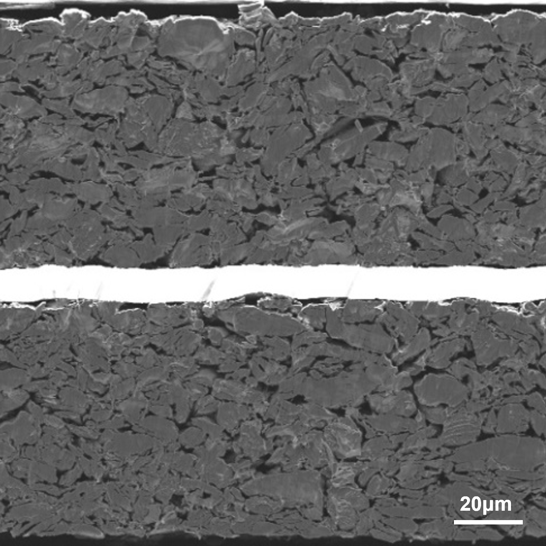


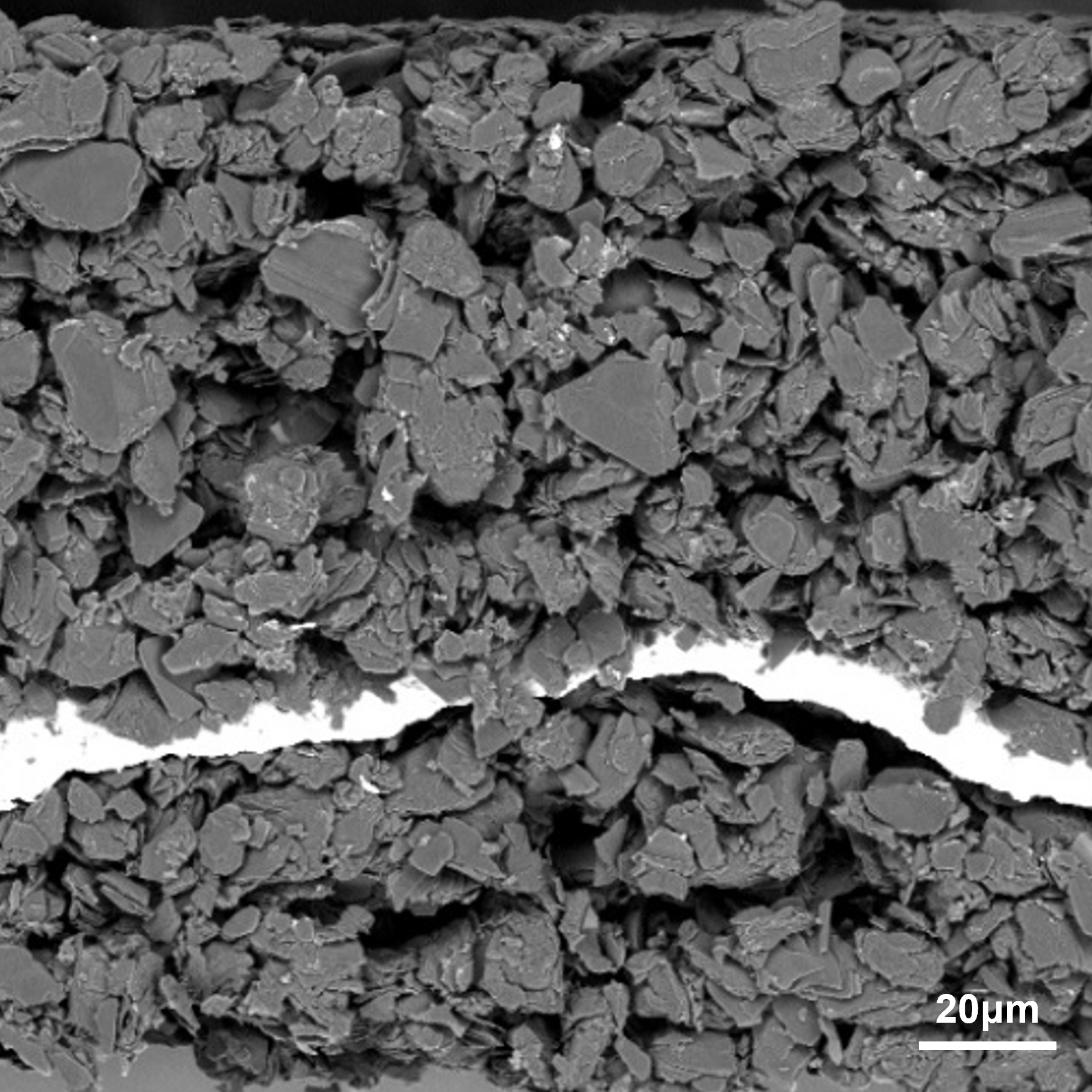
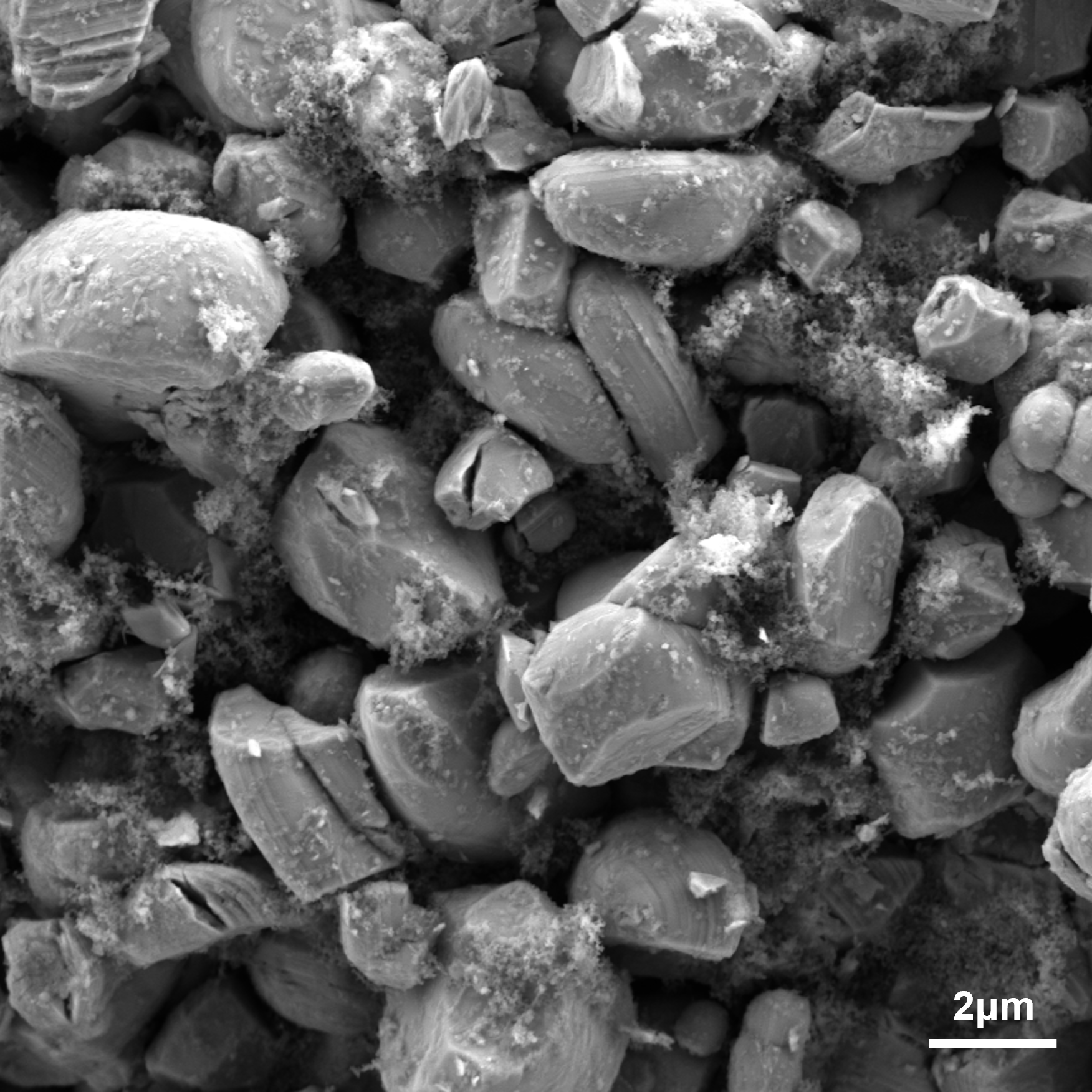
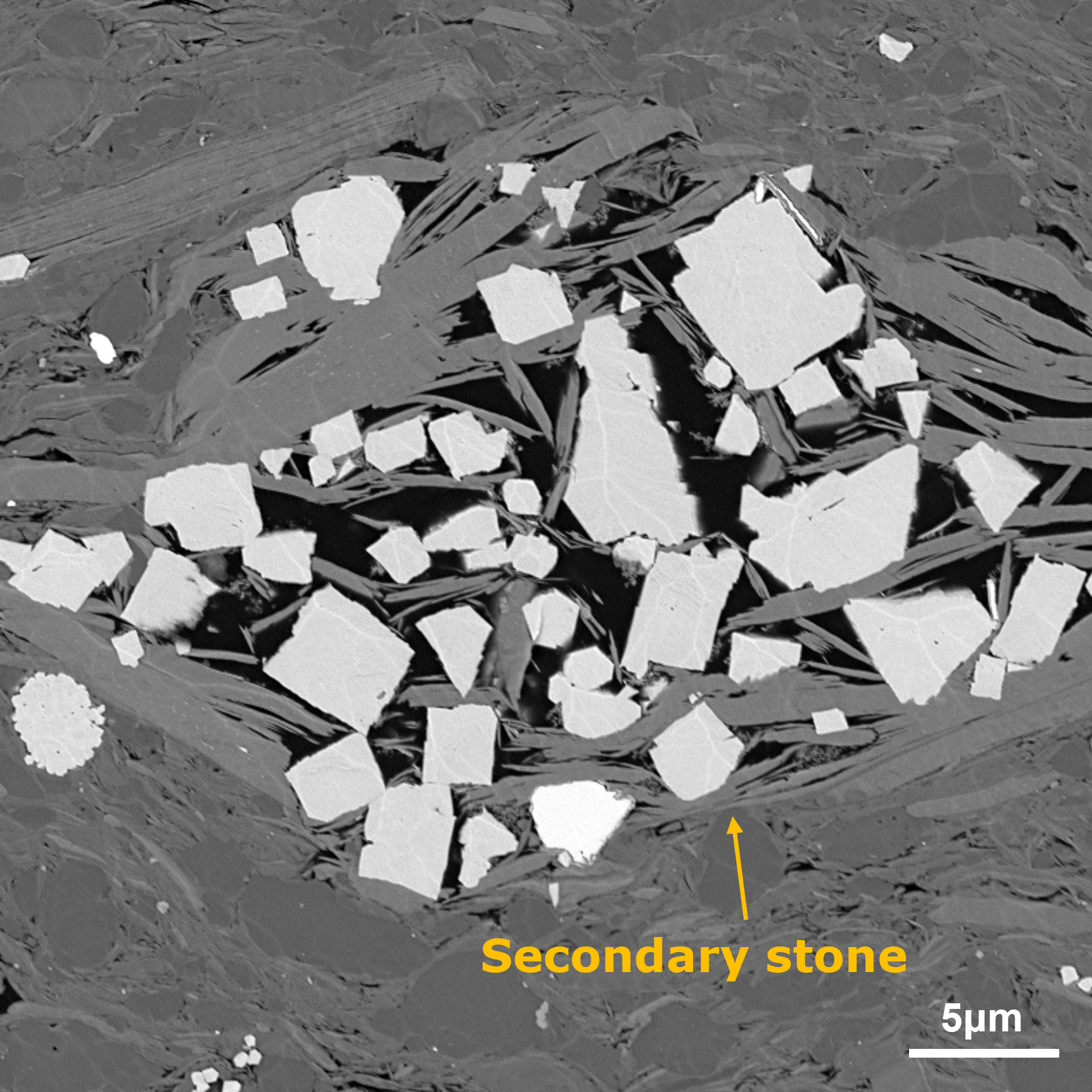
The image above is the secondary electron image after mechanical shear. It can be seen that due to the influence of shear force, the layers are not clear enough to make accurate measurement and obtain effective information. The image below shows the backscattered electron image of ABSEM200 after polishing, which allows accurate measurement of particle size and other information, and detailed study of the interface structure and composition. The picture above shows the secondary electron image of the ternary lithium electrode sheet, and the picture below shows the backscattered electron image after polishing ABSEM200. The picture above shows the secondary electron image of the lithium iron phosohate electrode sheet and the picture below shows the backscattered electron image after polishing ABSEM200. Petrogeology
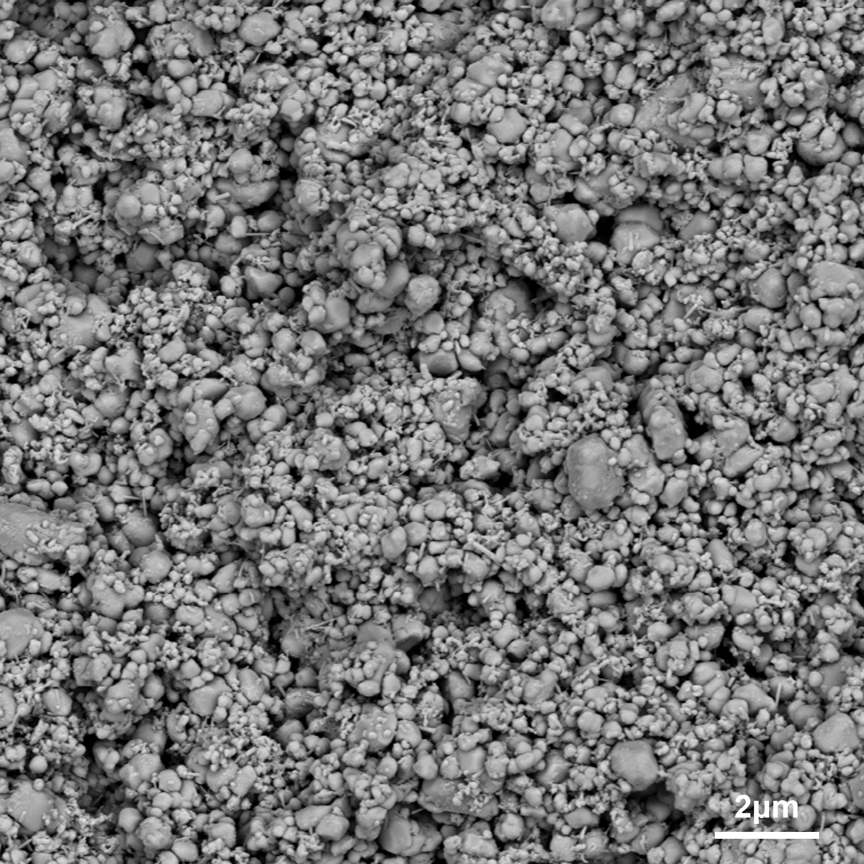
Oil scale After ion beam polishing 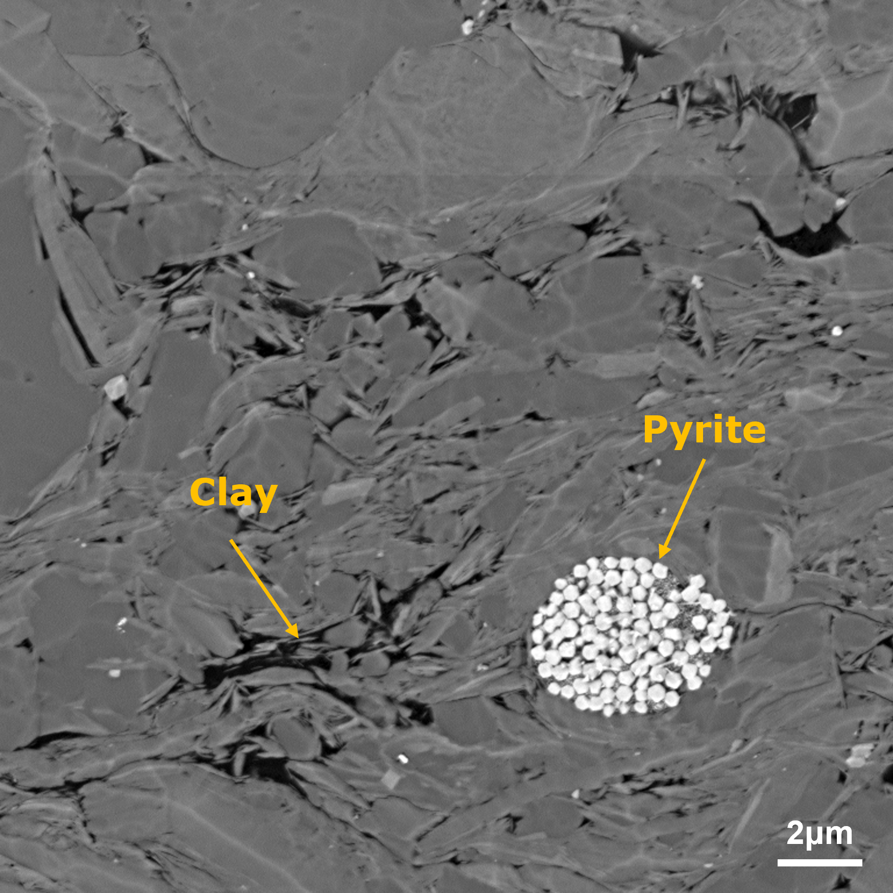
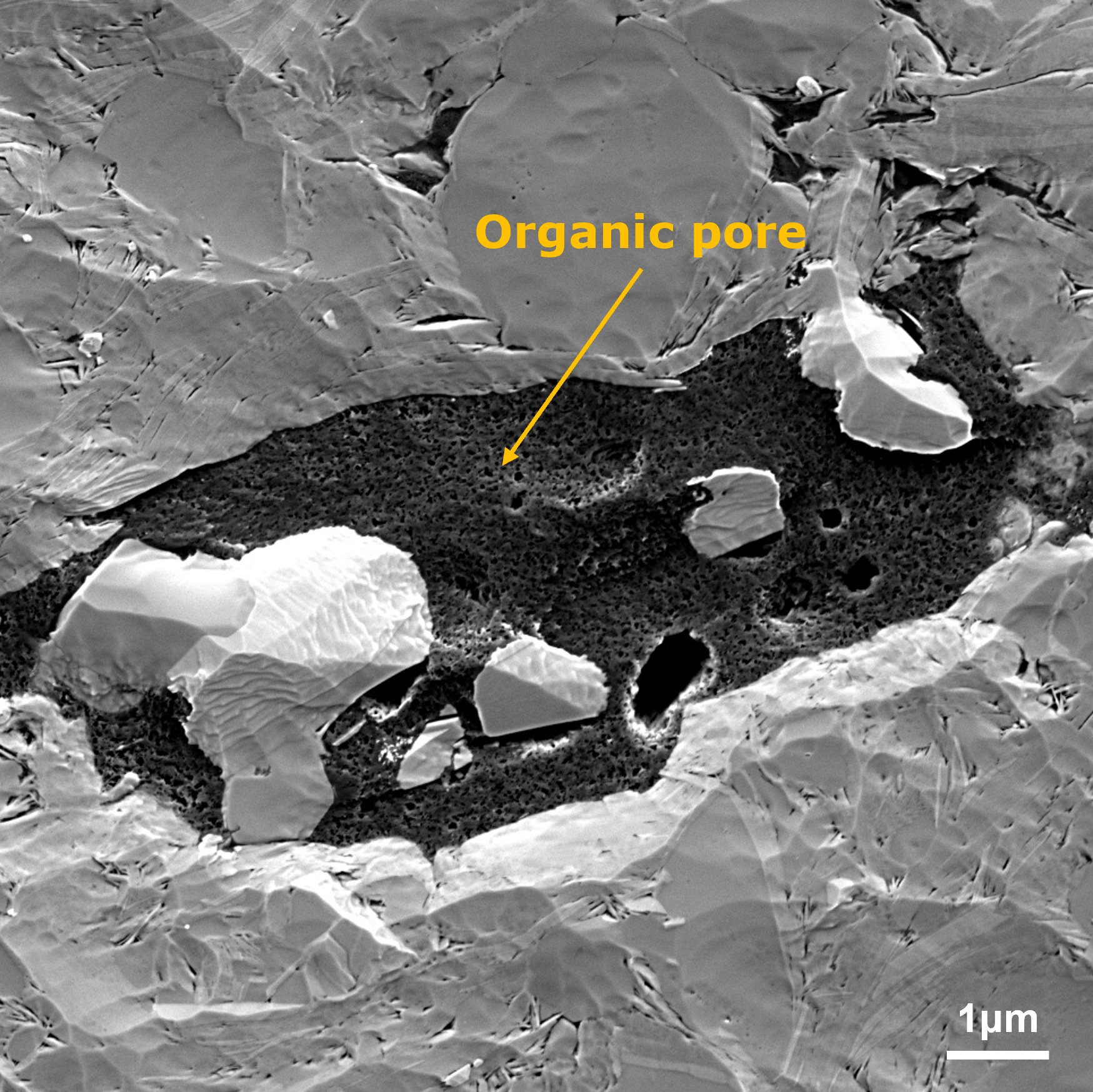
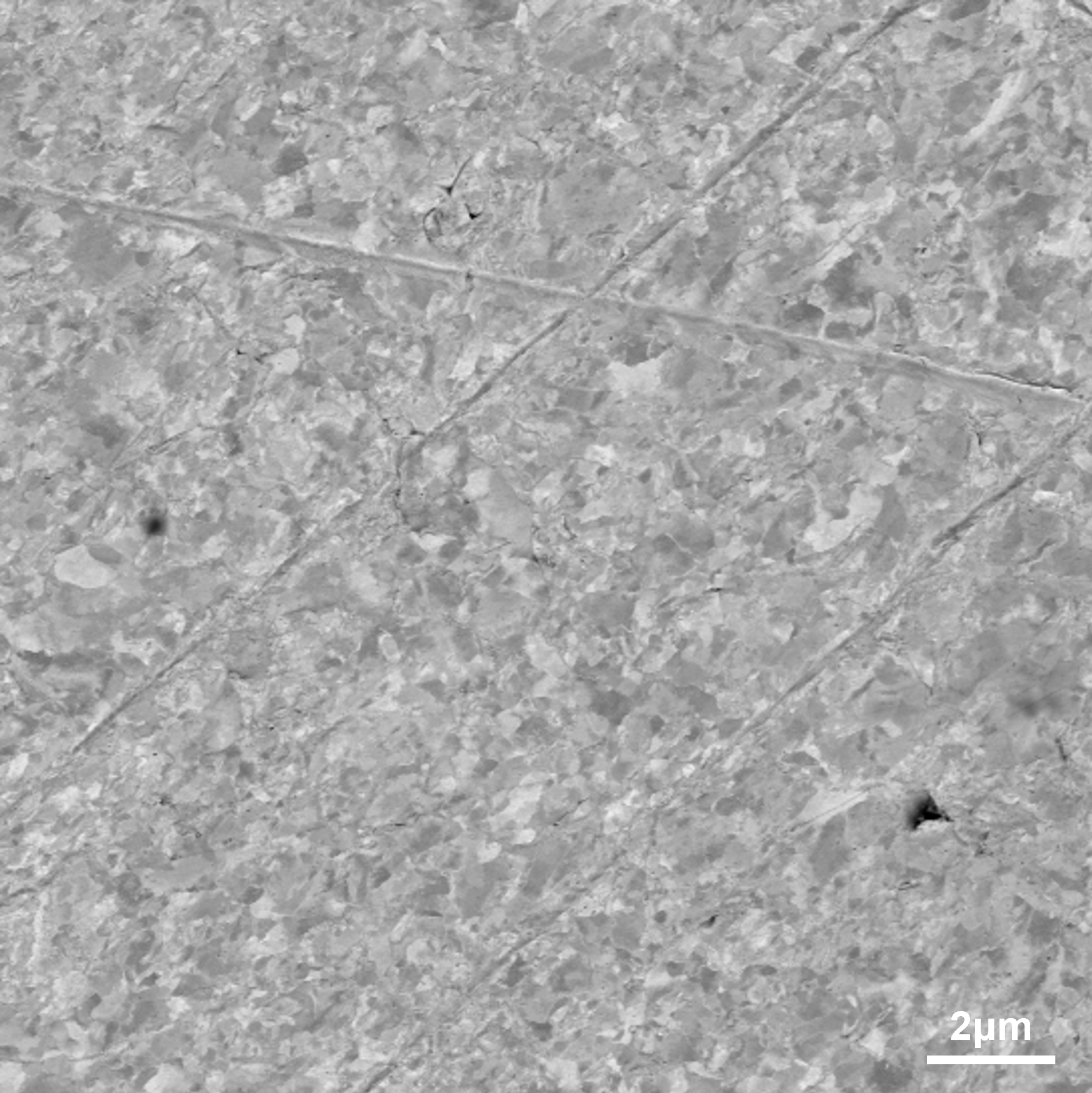
Before ion beam polishing, due to the different hardness of oil shale components, the surface quality is not good enough to obtain effective structural information. After polishing with ABSEM200, a flat surface can be obtained, exposing more details, such as the distribution of carbonates, silicates, pyrite, organic pores and other organics. Metallic material
Molybdenum After
mechanical
polishing
After ion beam polishing 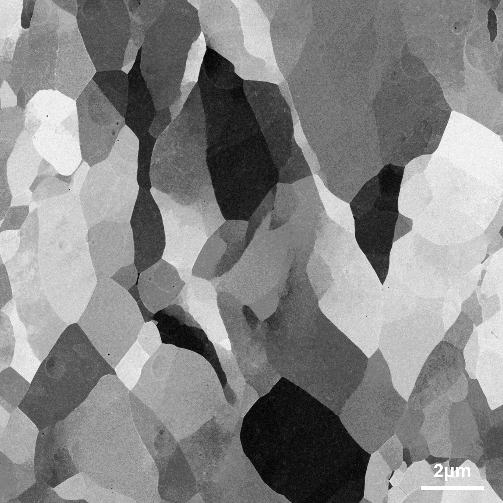
EBSD image 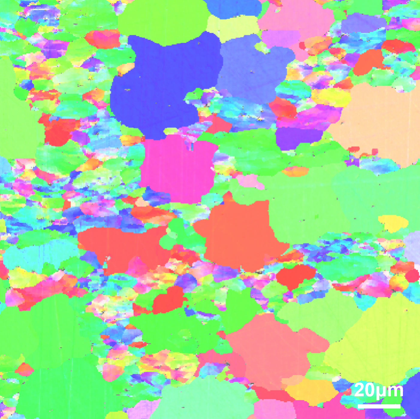
After mechanical polishing, there are many small scratches on the surface of molybdenum; After polishing with ABSEM200, backscattered electron imaging was performed, and the crystal orientation of the material was different. The grain boundaries of different crystal orientations can be directly observed thought electronic channel contrast, which is convenient for the statistics of grain size and orientation. Life sciences
Mouse cerebral cortex 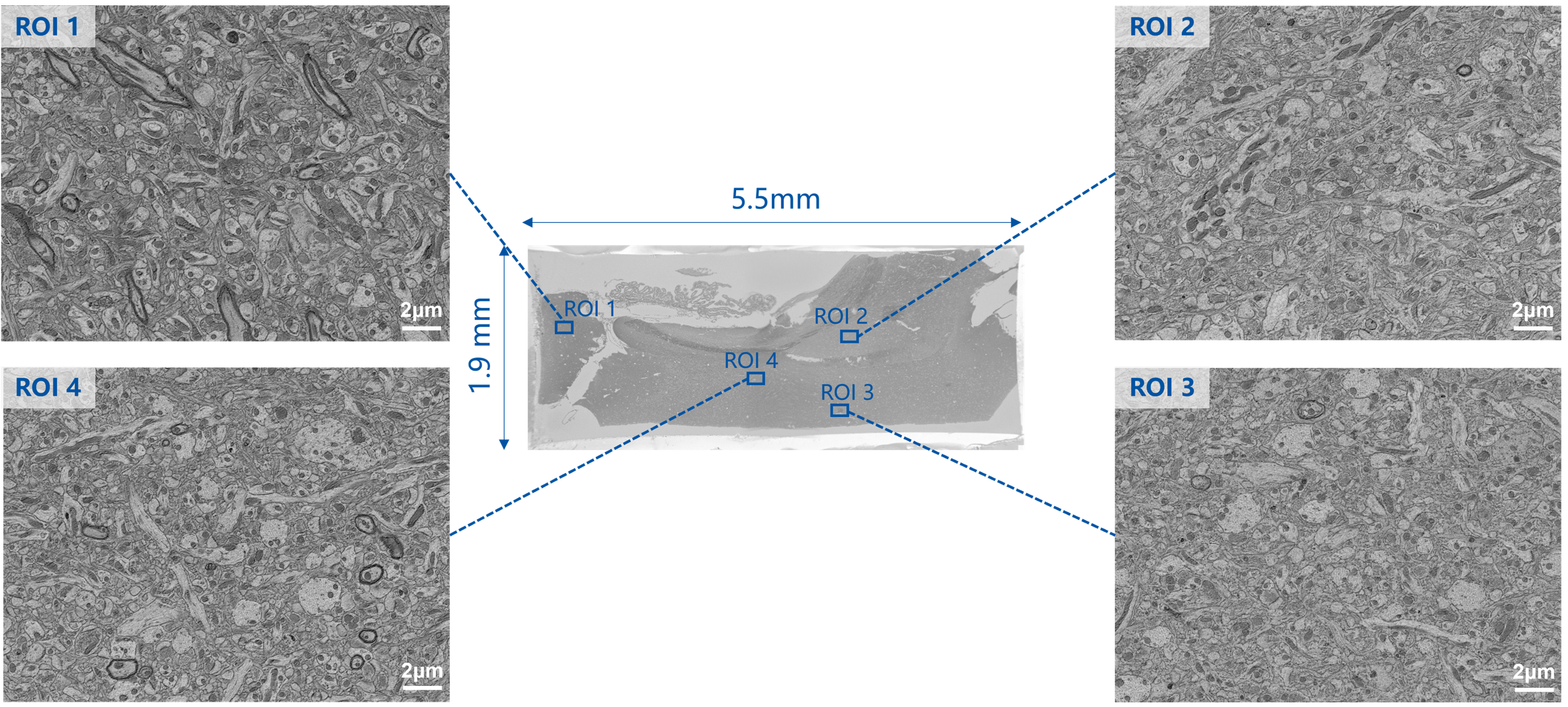
A flat surface was obtained by surface polishing of large scale (x: 5.5mm, y: 1.9mm) mouse cerebralcortex tissues with ABSEM200. The ultrastructural information of nerve tissue without ion damage can be seen by low-voltage backscattering electron imaging in different regions after polishing.
*The samples were obtained from Prof. Zhang Ruobing of Suzhou
Institute of Biomedical Engineering, Chinese Academy of Sciences.Zebrafish larvae torso 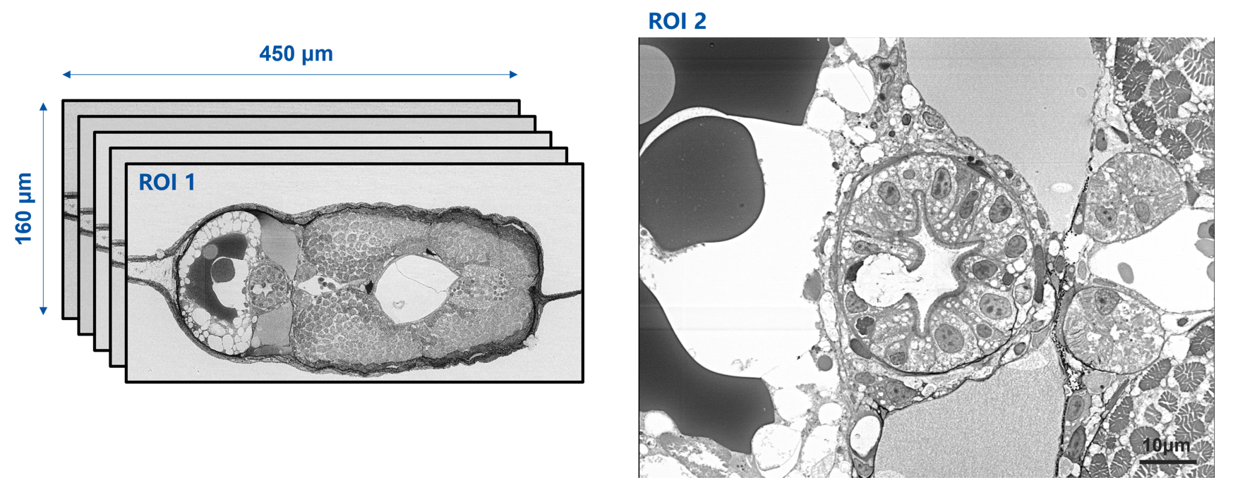
The complete zebrafish trunk was cut continuously with ABSEM200, and the image was imagnated with low-voltage backscatter electron detector, which can obtain the image with great contrast, high resolution and large field of view. The complete cell structure can be analyzed through semi-automatic collection of multiple continuous images. *The sample is obtained from Prof. Manfred Auer of Southeast University.
Performance parameters
- 产品描述
- 用户界面
- 性能参数
- 应用案例
-
- Commodity name: Argon ion field emission scanning electron microscope ABSEM200
As an innovative multi-functional sample preparation and analysis system,the argon ion beam field emission scanning electron microscope ABSEM 200 has made a breakthrough by integrating a broad-beam argon ion gun into into the scanning electron microscope. It has successfully achieved a seamless connection between ion beam in-situ polishing and high-resolution electron scanning imaging, eliminating sample transfer and greatly enhancing the analysis efficiency. The broad ion beam technology equipped on the ABSEM 200 has powerrul processing capabilities, enabling it to easily handle large-sized samples at the millimeter level, which significantly broadens its application range. The grazing angle design can effectively reduce the damage to samples during the processing, ensuring the integrity and original state of the samples. The nanometer-level layer cutting module can precisely control the layer removal thickness, and the unique debris trapping device ensures the stable operation of the system, effectively avoiding the interrerence of debris on experiments and potential risks.The ABSEM 200 is parricularly suitable for samples that are environmentally sensitive or have complex structures, providing users with an efficient and accurate sample characterization solution. The ABSEM 200 has successfully opened a new chapter in exploring the microscopic world!
Technical Principle
The ABSEM 200 dual beam system integrates the argon ion gun on the Yidon Technologies field emission scanning electron microscope platform, which makes the wide argon ion beam incident on the sample surrace at an adjustable grazing Angle (3-9°), and focuses the ion beam into a linear beam spot through the unidirectional focusing module at the front end to improve the beam density on the sample surface. The energy of the ion beam can be more efffciently applied to the microscopic region of the sample. The swing or rotation of the stage can effectively reduce the curtain effect and minimize the radiation damage of the sample. The ABSEM 200 is also equipped with a high-precision baffle layer cutting module, which can precisely remove the thickness of the sample surface according to the specific needs of the researchers, resulting in the ideal depth of observation and high-resolution resolution. At the same time, the unique debris capture device can effectively collect all kinds of pollutants generated in the ion beam sputtering, ensuring the clean and stable operating environment of the system. After the polishing process, the exposed sample surface can be directly scanned by high-resolution imaging without sample transfer, and the micro-morphology and structure information of the sample surface can be obtained.
Product Advantages
-
· Clear and concise interface layout
· Ergonomic keyboard design
· Equipped with multiple safety interlocks
· Simple and smooth operation
-
Ion-optical system
Ion beam energy range 0.5kV-5kV Ion beam current 10-500μA Beam spot diameter 0.3-10mm Gas type Ar Common air pressure 5e-5mbar Incident angle 3-9° Sample size and requirements for ion beam processing Specimen size ≤12mmx12mmx5mm Specimen weight ≤300g Layer cut range ≤200μm Layer cut stepping ≥8nm Electron-optical system Gun type Schottky FEG Acceleration voltage 0.02-30kV Probe current 1pA-20nA(100nA optionak configuration) Magnification 1-2,000,000x Resolution 1.0nm@15kV(SE),1.5nm@1kV(SE) Detector Standard configuration ET detector Inlens detector Optional configuration BSE detector Low-voltage BSE detector Specimen chamber Chamber 340mm inner diameter, 260mm height Automatic debris capture device Multiple accessory ports for EBSD, EDS, plasma cleaner, etc. Stage 5-axes automatic stage X、Y=125mm,Z=50mm,R=360° cont.,T=-5~70° Image system Top-view camera, side-view camera, argon ion beam monitoring Software Language Chinese/English, other languages can be customized System Windows Image size 512*512-16k*16k Automatic functions Automatic focus, automatic brightness/contrast, etc. Parameter recommendation Preset polishing parameters for common materials. Other functions Spilt screen display, image annotation and measurement, image blending, large-area image acquisition and stitching,etc. -
Energy battery
Graphite electrode sheet Ternary lithium electrode sheet Lithium iron phosphate electrode sheet
Before ion beam polishing
After ion beam polishing
The image above is the secondary electron image after mechanical shear. It can be seen that due to the influence of shear force, the layers are not clear enough to make accurate measurement and obtain effective information. The image below shows the backscattered electron image of ABSEM200 after polishing, which allows accurate measurement of particle size and other information, and detailed study of the interface structure and composition. The picture above shows the secondary electron image of the ternary lithium electrode sheet, and the picture below shows the backscattered electron image after polishing ABSEM200. The picture above shows the secondary electron image of the lithium iron phosohate electrode sheet and the picture below shows the backscattered electron image after polishing ABSEM200. Petrogeology
Oil scale After ion beam polishing Before ion beam polishing, due to the different hardness of oil shale components, the surface quality is not good enough to obtain effective structural information. After polishing with ABSEM200, a flat surface can be obtained, exposing more details, such as the distribution of carbonates, silicates, pyrite, organic pores and other organics. Metallic material
Molybdenum After
mechanical
polishing
After ion beam polishing EBSD image After mechanical polishing, there are many small scratches on the surface of molybdenum; After polishing with ABSEM200, backscattered electron imaging was performed, and the crystal orientation of the material was different. The grain boundaries of different crystal orientations can be directly observed thought electronic channel contrast, which is convenient for the statistics of grain size and orientation. Life sciences
Mouse cerebral cortex A flat surface was obtained by surface polishing of large scale (x: 5.5mm, y: 1.9mm) mouse cerebralcortex tissues with ABSEM200. The ultrastructural information of nerve tissue without ion damage can be seen by low-voltage backscattering electron imaging in different regions after polishing.
*The samples were obtained from Prof. Zhang Ruobing of Suzhou
Institute of Biomedical Engineering, Chinese Academy of Sciences.Zebrafish larvae torso The complete zebrafish trunk was cut continuously with ABSEM200, and the image was imagnated with low-voltage backscatter electron detector, which can obtain the image with great contrast, high resolution and large field of view. The complete cell structure can be analyzed through semi-automatic collection of multiple continuous images. *The sample is obtained from Prof. Manfred Auer of Southeast University.
Application Cases
- 产品描述
- 用户界面
- 性能参数
- 应用案例
-
- Commodity name: Argon ion field emission scanning electron microscope ABSEM200
As an innovative multi-functional sample preparation and analysis system,the argon ion beam field emission scanning electron microscope ABSEM 200 has made a breakthrough by integrating a broad-beam argon ion gun into into the scanning electron microscope. It has successfully achieved a seamless connection between ion beam in-situ polishing and high-resolution electron scanning imaging, eliminating sample transfer and greatly enhancing the analysis efficiency. The broad ion beam technology equipped on the ABSEM 200 has powerrul processing capabilities, enabling it to easily handle large-sized samples at the millimeter level, which significantly broadens its application range. The grazing angle design can effectively reduce the damage to samples during the processing, ensuring the integrity and original state of the samples. The nanometer-level layer cutting module can precisely control the layer removal thickness, and the unique debris trapping device ensures the stable operation of the system, effectively avoiding the interrerence of debris on experiments and potential risks.The ABSEM 200 is parricularly suitable for samples that are environmentally sensitive or have complex structures, providing users with an efficient and accurate sample characterization solution. The ABSEM 200 has successfully opened a new chapter in exploring the microscopic world!
Technical Principle
The ABSEM 200 dual beam system integrates the argon ion gun on the Yidon Technologies field emission scanning electron microscope platform, which makes the wide argon ion beam incident on the sample surrace at an adjustable grazing Angle (3-9°), and focuses the ion beam into a linear beam spot through the unidirectional focusing module at the front end to improve the beam density on the sample surface. The energy of the ion beam can be more efffciently applied to the microscopic region of the sample. The swing or rotation of the stage can effectively reduce the curtain effect and minimize the radiation damage of the sample. The ABSEM 200 is also equipped with a high-precision baffle layer cutting module, which can precisely remove the thickness of the sample surface according to the specific needs of the researchers, resulting in the ideal depth of observation and high-resolution resolution. At the same time, the unique debris capture device can effectively collect all kinds of pollutants generated in the ion beam sputtering, ensuring the clean and stable operating environment of the system. After the polishing process, the exposed sample surface can be directly scanned by high-resolution imaging without sample transfer, and the micro-morphology and structure information of the sample surface can be obtained.
Product Advantages
-
· Clear and concise interface layout
· Ergonomic keyboard design
· Equipped with multiple safety interlocks
· Simple and smooth operation
-
Ion-optical system
Ion beam energy range 0.5kV-5kV Ion beam current 10-500μA Beam spot diameter 0.3-10mm Gas type Ar Common air pressure 5e-5mbar Incident angle 3-9° Sample size and requirements for ion beam processing Specimen size ≤12mmx12mmx5mm Specimen weight ≤300g Layer cut range ≤200μm Layer cut stepping ≥8nm Electron-optical system Gun type Schottky FEG Acceleration voltage 0.02-30kV Probe current 1pA-20nA(100nA optionak configuration) Magnification 1-2,000,000x Resolution 1.0nm@15kV(SE),1.5nm@1kV(SE) Detector Standard configuration ET detector Inlens detector Optional configuration BSE detector Low-voltage BSE detector Specimen chamber Chamber 340mm inner diameter, 260mm height Automatic debris capture device Multiple accessory ports for EBSD, EDS, plasma cleaner, etc. Stage 5-axes automatic stage X、Y=125mm,Z=50mm,R=360° cont.,T=-5~70° Image system Top-view camera, side-view camera, argon ion beam monitoring Software Language Chinese/English, other languages can be customized System Windows Image size 512*512-16k*16k Automatic functions Automatic focus, automatic brightness/contrast, etc. Parameter recommendation Preset polishing parameters for common materials. Other functions Spilt screen display, image annotation and measurement, image blending, large-area image acquisition and stitching,etc. -
Energy battery
Graphite electrode sheet Ternary lithium electrode sheet Lithium iron phosphate electrode sheet
Before ion beam polishing
After ion beam polishing
The image above is the secondary electron image after mechanical shear. It can be seen that due to the influence of shear force, the layers are not clear enough to make accurate measurement and obtain effective information. The image below shows the backscattered electron image of ABSEM200 after polishing, which allows accurate measurement of particle size and other information, and detailed study of the interface structure and composition. The picture above shows the secondary electron image of the ternary lithium electrode sheet, and the picture below shows the backscattered electron image after polishing ABSEM200. The picture above shows the secondary electron image of the lithium iron phosohate electrode sheet and the picture below shows the backscattered electron image after polishing ABSEM200. Petrogeology
Oil scale After ion beam polishing Before ion beam polishing, due to the different hardness of oil shale components, the surface quality is not good enough to obtain effective structural information. After polishing with ABSEM200, a flat surface can be obtained, exposing more details, such as the distribution of carbonates, silicates, pyrite, organic pores and other organics. Metallic material
Molybdenum After
mechanical
polishing
After ion beam polishing EBSD image After mechanical polishing, there are many small scratches on the surface of molybdenum; After polishing with ABSEM200, backscattered electron imaging was performed, and the crystal orientation of the material was different. The grain boundaries of different crystal orientations can be directly observed thought electronic channel contrast, which is convenient for the statistics of grain size and orientation. Life sciences
Mouse cerebral cortex A flat surface was obtained by surface polishing of large scale (x: 5.5mm, y: 1.9mm) mouse cerebralcortex tissues with ABSEM200. The ultrastructural information of nerve tissue without ion damage can be seen by low-voltage backscattering electron imaging in different regions after polishing.
*The samples were obtained from Prof. Zhang Ruobing of Suzhou
Institute of Biomedical Engineering, Chinese Academy of Sciences.Zebrafish larvae torso The complete zebrafish trunk was cut continuously with ABSEM200, and the image was imagnated with low-voltage backscatter electron detector, which can obtain the image with great contrast, high resolution and large field of view. The complete cell structure can be analyzed through semi-automatic collection of multiple continuous images. *The sample is obtained from Prof. Manfred Auer of Southeast University.
Customer service telephone
Enterprise mailbox
Company address
88, Keling Road, Suzhou New District, Jiangsu Province, 215163, China
Copyright©2023 Yidon Technologies (Suzhou) Co., Ltd. All rights reserved Website Construction:China Enterprise Power Kunshan SEO