

News
Embarking on a New Journey, Revealing the Extraordinary ——Yidon Technologies Launches Two New Field Emission Scanning Electron Microscopes
12-30
On the morning of December 24th, Yidon Technologies held an online product launch event themed "Embarking on a New Journey, Revealing the Extraordinary" on the Instrument Information Network. It introduced the new-generation field emission scanning electron microscope YF-2800 and the argon ion beam field emission scanning electron microscope ABSEM 200, attracting hundreds of listeners from various universities, research institutes, and industrial enterprises to communicate and learn. The event received a warm response.
1、Field Emission Scanning Electron Microscope YF-2800
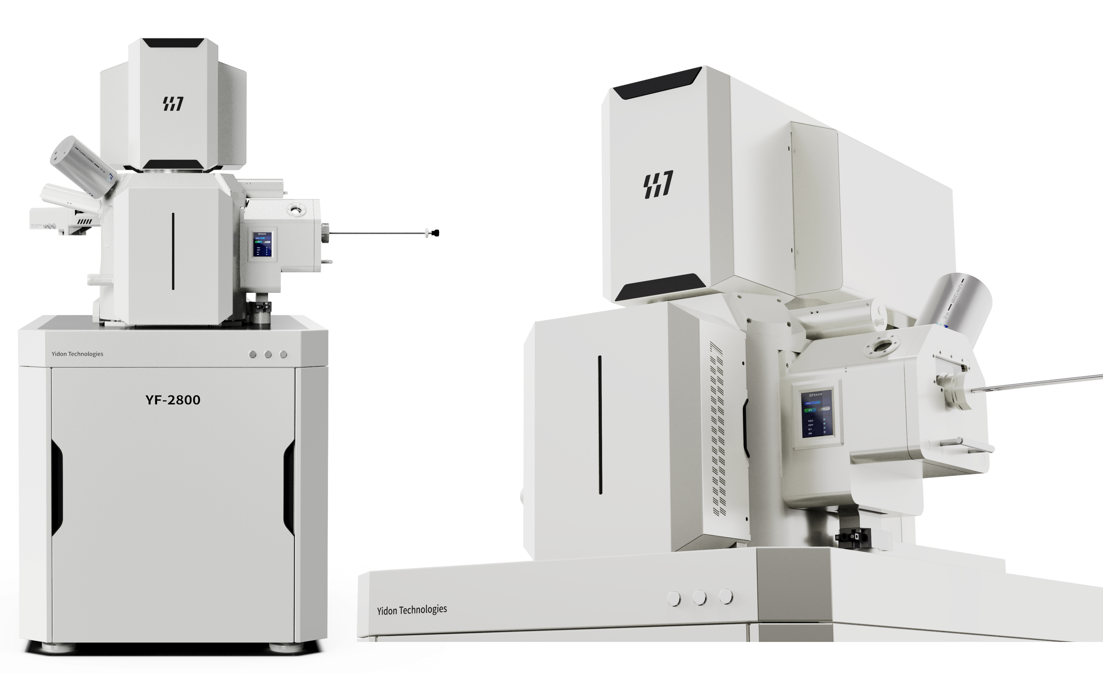
The YF-2800 scanning electron microscope of Yidong Optics boasts outstanding low-voltage high-resolution imaging capabilities (with a resolution reaching 0.8nm @ 15kV and 1.2nm @ 1kV). It is equipped with a thermal field emission electron gun (Schottky FEG), ensuring the stability of the beam current while achieving high resolution. Advanced in-column acceleration technology has been incorporated into the electron optical design, guaranteeing excellent imaging performance of the electron beam under low acceleration voltages. The immersion magnetic objective lens design is adopted to further enhance the high-resolution imaging ability of the system. The optimized detection system can efficiently collect secondary electron and backscattered electron signals at low voltages. It enables direct observation of non-conductive samples at low voltages, reduces irradiation damage to samples, and reveals the surface microscopic morphology and structural information of samples.
2、Argon Ion Beam Field Emission Scanning Electron Microscope ABSEM 200

The argon ion beam field emission scanning electron microscope ABSEM 200, as an innovative multi-functional sample preparation and analysis system, has made a breakthrough by integrating a broad-beam argon ion gun into the sample chamber of the scanning electron microscope. It has successfully achieved seamless integration between ion beam in-situ polishing and high-resolution electron beam imaging analysis, eliminating the need for cumbersome sample transfer processes and greatly improving the analysis efficiency.
The broad ion beam technology equipped on the ABSEM 200 has powerful processing capabilities and can easily handle large-sized samples at the millimeter level, which significantly broadens its application range. The grazing angle design can effectively reduce the damage to samples during the processing, ensuring the integrity and original state of the samples. The nanometer-level layer cutting module can precisely control the layer removal thickness, and the unique debris trapping device ensures the stable operation of the system, effectively avoiding the interference of debris on experiments and potential risks.
The ABSEM 200 is particularly suitable for samples that are environmentally sensitive or have complex structures, providing users with an efficient and accurate sample characterization solution. The ABSEM 200 has successfully opened a brand-new chapter in exploring the microscopic world!
Previous
Dec 04,2025
Oct 10,2025
Oct 10,2025
Customer service telephone
Enterprise mailbox
Company address
88, Keling Road, Suzhou New District, Jiangsu Province, 215163, China
Copyright©2023 Yidon Technologies (Suzhou) Co., Ltd. All rights reserved Website Construction:China Enterprise Power Kunshan SEO